
In a development that underscores the future of computing, NVIDIA has poured a staggering $6.5 billion into the silicon photonics sector since March 2026. This aggressive financial push is aimed squarely at replacing traditional copper wiring with light-based technology, a change deemed essential for the next generation of AI data centers. While the promise is a future of unparalleled data speeds and lower energy use, the reality is far more complex and fraught with risk. The central question is whether this expensive bet on the technology will pay off, or if it exposes a critical vulnerability in the AI hardware ecosystem.
Table of Contents
 (https://substackcdn.com/image/fetch/$s_!zy4P!,f_auto,q_auto:good,fl_progressive:steep/https%3A%2F%2Fsubstack-post-media.s3.amazonaws.com%2Fpublic%2Fimages%2Fc6270241-79e5-45f2-9baf-ae32b834db52_2310x1302.png)
Decoding Nvidia’s High-Stakes Ecosystem Play
To grasp the magnitude of this move, one must look at the intricate supply chain for this innovation. This goes far beyond one breakthrough; it’s a calculated effort to control an entire ecosystem. The investments are spread across several key players, each holding a crucial piece of the puzzle. Major stakes in companies like Lumentum and Coherent Corp. secure access to the essential laser and optical component manufacturing that forms the heart of the system technology.
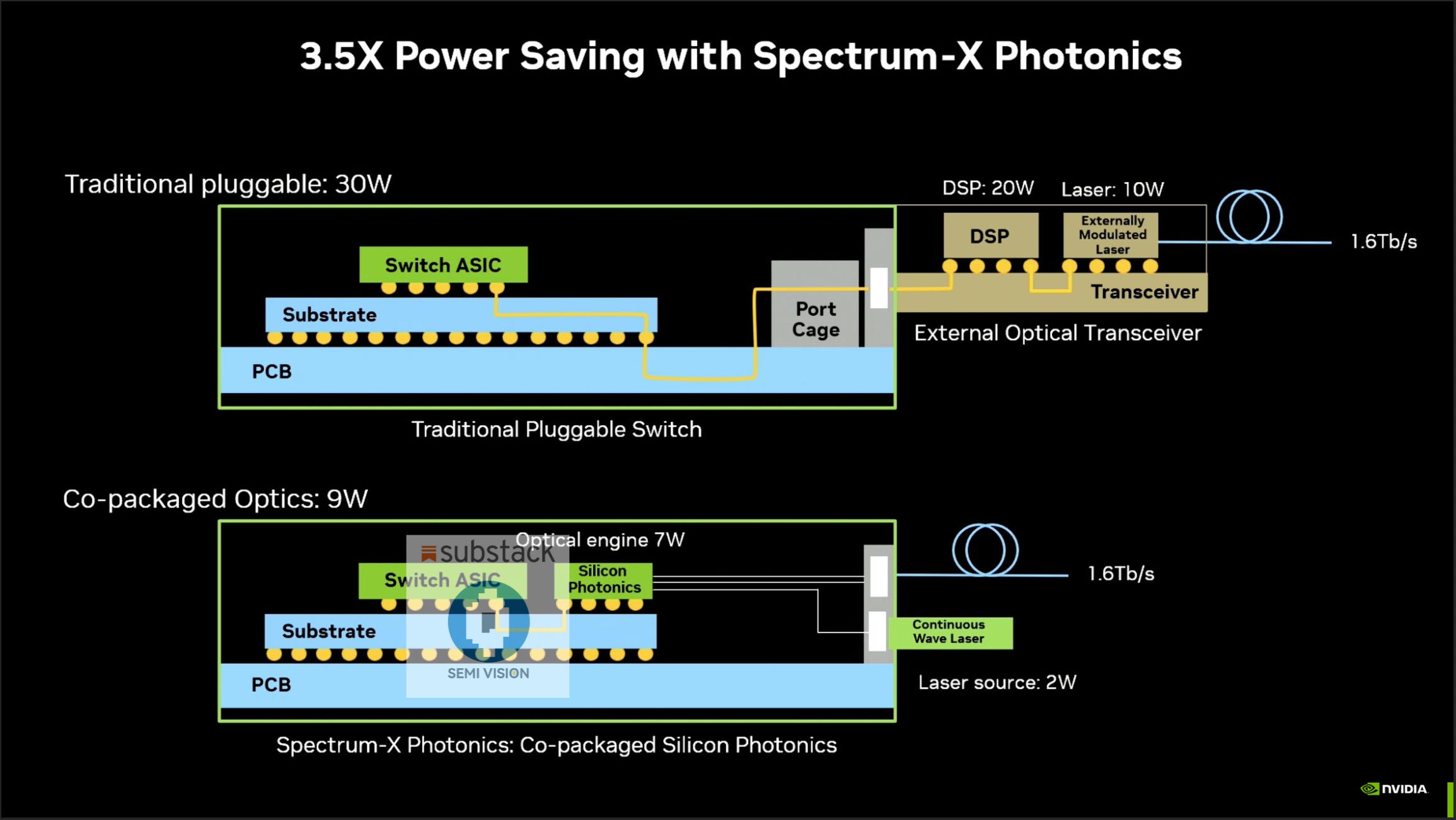
Additionally, funding for firms like Marvell Technology and Corning points to a strategy of vertical integration, controlling everything from the specialized chips to the fiber optics they connect to. The real gem in this portfolio might be Ayar Labs, a startup specializing in co-packaged optics—integrating it directly with the processor. This approach promises to dramatically reduce latency and power consumption, which are the primary bottlenecks holding back the scaling of massive AI models. The technical moat is the highly complex process of manufacturing these components at scale with high yields, a problem the industry has been wrestling with for over a decade.
Also read: Compute-in-memory: The Critical Bottleneck Stalling AI’s Future
Scrutinizing the Claims Behind the silicon photonics Hype
The marketing pitch suggests that the platform is a miracle cure for the data jams plaguing modern AI clusters. Nvidia’s vision, articulated through these investments, is a future where data flows as light, obliterating the energy waste and bandwidth limits of copper interconnects. The goal is to enable GPU clusters that are orders of magnitude more powerful than today’s, a necessary step for training tomorrow’s AI. Ayar Labs, for instance, has showcased its optical I/O solution as a way to achieve terabit-per-second bandwidths at a fraction of the power of electrical I/O.
However, our investigation reveals a more troubled picture. Industry insiders whisper that production yields for complex photonic integrated circuits remain stubbornly problematic. The cost of fabricating and packaging these light-based chips is still prohibitively high compared to traditional methods, which could delay widespread adoption. While Nvidia is building a “dream team” of suppliers, the technological maturity isn’t yet guaranteed. This gap between the advertised performance of the technology and the current, real-world manufacturing capability represents a dangerous risk to Nvidia’s roadmap.
Regulatory and Competitive Friction in the Photonics Race
A critical long-term risk of Nvidia’s strategy is the centralization of a technology as fundamental as this innovation. By buying significant stakes in the few companies that can produce these components at a high level, NVIDIA is creating a powerful dependency. This level of control could give one company immense leverage over the entire AI industry, from cloud providers to rival chipmakers. The success of future AI development would hinge on the manufacturing success and pricing decisions of a handful of firms heavily influenced by Nvidia.
This emerging dynamic is raising alarms. Analysts at major tech research firms are beginning to question the long-term implications. The concentration of the the system supply chain presents a fragile single point of failure. Any disruption—be it geopolitical, a manufacturing flaw, or a natural disaster affecting a key facility—could halt progress for the entire industry. This is the opposite of the more diversified and resilient supply chains that have characterized the semiconductor industry for decades, creating a new and concerning vector of risk for the future of it.
Related article: Wafer-to-wafer hybrid bonding: A Critical Breakthrough or Just More Hype?
The Bottom Line on silicon photonics
Ultimately: Nvidia’s multi-billion-dollar investment in the platform is not merely a strategic choice; it is an act of necessity. The company recognizes that without a radical shift away from copper, the progress of AI will hit a hard physical wall. The move to consolidate the supply chain is a high-risk, high-reward gambit to ensure its dominance continues in the AI era. While the technology is undeniably the future, its present is fraught with manufacturing hurdles and strategic vulnerabilities that cannot be ignored.
Critical Signals to Watch:
- Watch for: Publicly reported manufacturing yield rates from Lumentum and Coherent. Any significant drop or stagnation is a red flag.
- A critical sign: The pace of adoption for co-packaged optics by other major players like AMD, Intel, or Google. A lack of broader uptake could signal that the technology is not yet ready for primetime.
- Look for: The emergence of new, independent startups in the this innovation space that are not tied to Nvidia’s investment portfolio. True competition is a sign of a healthy ecosystem.
- An important signal: Any regulatory scrutiny from trade commissions in the US or EU regarding supply chain concentration in the photonics sector.
- Indicator to track: The cost-per-gigabit of optical interconnects versus electrical ones. The crossover point where silicon photonics becomes economically viable at scale is the ultimate tipping point.
As of today, silicon photonics remains a technology of immense promise but equally immense risk. Nvidia has placed its bet, and the entire tech world is waiting to see if it pays off.